- 您现在的位置:买卖IC网 > Sheet目录342 > MIC2287-34YML TR (Micrel Inc)IC LED DRIVER WHITE BCKLGT 8-MLF
MIC2287
Absolute Maximum Ratings (1)
Supply Voltage (V IN ) ..................................................... 12V
Switch Voltage (V SW ) ......................................–0.3V to 34V
Enable Pin Voltage (V EN ) ................................... –0.3 to V IN
FB Voltage (V FB ) ............................................................. 6V
Switch Current (I SW ) ........................................................ 2A
Ambient Storage Temperature (T S ) .......... –65°C to +150°C
ESD Rating (3) ............................................................... 2kV
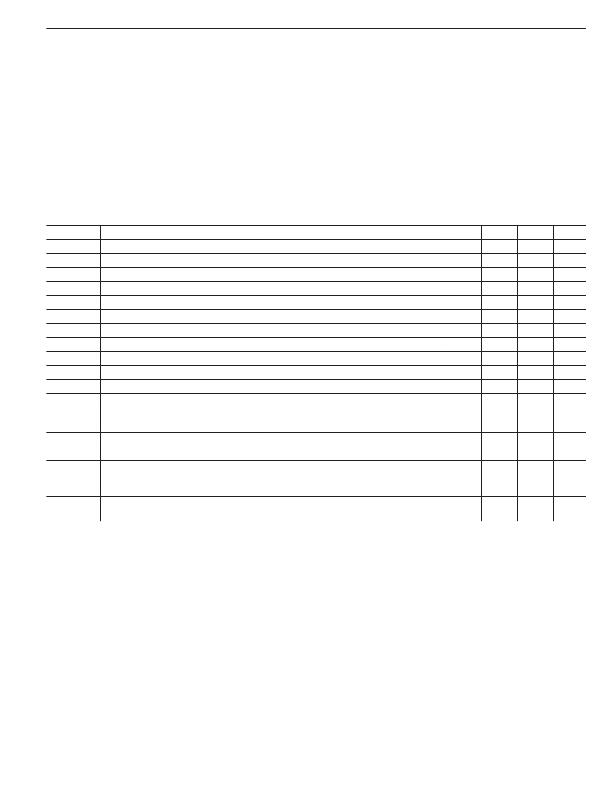
Electrical Characteristics (4)
Micrel, Inc.
Operating Ratings (2)
Supply Voltage (V IN ) ..........................................2.5V to 10V
Junction Temperature Range (T J ) ............ –40°C to +125°C
Package Thermal Impedance
2mm × 2mmMLF? ( θ JA ) ..................................... 93°C/W
Thin SOT-23-5 ( θ JA ) ......................................... 256°C/W
T A = 25°C, V IN = V EN = 3.6V, V OUT = 10V, I OUT = 10mA, unless otherwise noted. Bold values indicate –40°C ≤ T J ≤125°C.
Symbol Parameter Condition Min Typ Max
Units
V IN
V UVLO
I VIN
I SD
V FB
I FB
D MAX
I SW
V SW
I SW
V EN
I EN
f SW
V OVP
T J
Supply Voltage Range
Under Voltage Lockout
Quiescent Current
Shutdown Current
Feedback Voltage
Feedback Input Current
Line Regulation (6)
Load Regulation (6)
Maximum Duty Cycle
Switch Current Limit
Switch Saturation Voltage
Switch Leakage Current
Enable Threshold
Enable Pin Current
Oscillator Frequency
Overvoltage Protection
Overtemperature
Threshold Shutdown
V FB > 200mV, (not switching)
V EN = 0V (5)
(±5%)
V FB = 95mV
3V ≤ V IN ≤ 5V
5mA ≤ I OUT ≤ 20mA
I SW = 0.5A
V EN = 0V, V SW = 10V
TURN ON
TURN OFF
V EN = 10V
MIC2287BML- 15 only
MIC2287BML- 24 only
MIC2287BML- 34 only
Hysteresis
2.5
1.8
90
85
1.5
1.05
13
21
30
2.1
2.5
0.1
95
–450
0.5
0.5
90
750
450
0.01
20
1.2
14
22.5
32
150
10
10
2.4
5
1
100
1
2
5
0.4
40
1.35
16
24
34
V
V
mA
μA
mV
nA
%
%
%
mA
mV
μA
V
V
μA
MHz
V
V
V
°C
°C
Notes:
1. Absolute maximum ratings indicate limits beyond which damage to the component may occur. Electrical speci?cations do not apply when operating
the device outside of its operating ratings. The maximum allowable power dissipation is a function of the maximum junction temperature, T J (max),
the junction-to-ambient thermal resistance, θ JA , and the ambient temperature, T A . The maximum allowable power dissipation will result in excessive
die temperature, and the regulator will go into thermal shutdown.
2. This device is not guaranteed to operate beyond its speci?ed operating ratings.
3. Devices are inherently ESD sensitive. Handling precautions required. Human body model.
4. Speci?cation for packaged product only.
5. I SD = I VIN .
6. Guaranteed by design.
July 2005
3
M9999-070105
发布紧急采购,3分钟左右您将得到回复。
相关PDF资料
MIC2289C-34YD6 TR
IC LED DRIVR WHITE BCKLGT TSOT-6
MIC2291YD5 TR
IC LED DRIVER PHOTO FLASH TSOT-5
MIC2293-15YML TR
IC LED DRIVER WHITE BCKLGT 8-MLF
MIC2293C-34YML TR
IC LED DRIVER WHITE BCKLGT 8-MLF
MIC2297-42YML TR
IC LED DRIVR WHITE BCKLGT 10-MLF
MIC2298-15YML TR
IC LED DRIVER HIGH BRIGHT 12-MLF
MIC2299-15YML TR
IC LED DRIVR WHITE BCKLGT 12-MLF
MIC26603YJL EV
BOARD EVAL FOR MIC26603YJL
相关代理商/技术参数
MIC2287-34YML-TR
功能描述:LED 驱动器 IC 1 输出 DC DC 稳压器 升压(升压) 模拟,PWM 调光 750mA(开关) 8-MLF?(2x2) 制造商:microchip technology 系列:- 包装:剪切带(CT) 零件状态:停产 类型:DC DC 稳压器 拓扑:升压(升压) 内部开关:是 输出数:1 电压 - 供电(最低):2.5V 电压 -?供电(最高):10V 电压 - 输出:34V 电流 - 输出/通道:750mA(开关) 频率:1.2MHz 调光:模拟,PWM 应用:背光,照相机闪光灯 工作温度:-40°C ~ 125°C (TJ) 安装类型:表面贴装 封装/外壳:8-VFDFN 裸露焊盘,8-MLF? 供应商器件封装:8-MLF?(2x2) 标准包装:1
MIC2287-3-LED-EV
功能描述:MIC2287 1, Non-Isolated Output LED Driver Evaluation Board 制造商:microchip technology 系列:- 零件状态:无货 电流 - 输出/通道:- 输出和类型:1,非隔离 电压 - 输出:- 特性:- 电压 - 输入:2.5 V ~ 10 V 所含物品:板 使用的 IC/零件:MIC2287 标准包装:1
MIC2287-6-LED-EV
功能描述:MIC2287 1, Non-Isolated Output LED Driver Evaluation Board 制造商:microchip technology 系列:- 零件状态:无货 电流 - 输出/通道:- 输出和类型:1,非隔离 电压 - 输出:- 特性:- 电压 - 输入:2.5 V ~ 10 V 所含物品:板 使用的 IC/零件:MIC2287 标准包装:1
MIC2287BD5
制造商:MICREL 制造商全称:Micrel Semiconductor 功能描述:1.2MHz PWM White LED Driver with OVP in 2mm 】 2mm MLF⑩ and Thin SOT-23
MIC2287BD5 TR
功能描述:IC LED DRVR WHT BCKLGT TSOT23-5 RoHS:否 类别:集成电路 (IC) >> PMIC - LED 驱动器 系列:- 标准包装:1 系列:- 恒定电流:- 恒定电压:- 拓扑:PWM,切换式电容器(充电泵) 输出数:1 内部驱动器:是 类型 - 主要:背光 类型 - 次要:白色 LED 频率:642kHz 电源电压:2.7 V ~ 5.5 V 输出电压:5V 安装类型:表面贴装 封装/外壳:10-VFDFN 裸露焊盘 供应商设备封装:10-VSON 包装:剪切带 (CT) 工作温度:-30°C ~ 85°C 产品目录页面:1371 (CN2011-ZH PDF) 其它名称:BD1603NUV-E2CT
MIC2287C
制造商:MICREL 制造商全称:Micrel Semiconductor 功能描述:1.2MHz PWM White LED Driver with OVP in 2mm × 2mm MLF and Thin SOT-23
MIC2287C_11
制造商:MICREL 制造商全称:Micrel Semiconductor 功能描述:1.2MHz PWM White LED Driver with OVP in 2mm × 2mm MLF and Thin SOT-23
MIC2287C-15BML
制造商:MICREL 制造商全称:Micrel Semiconductor 功能描述:1.2MHz PWM White LED Driver with OVP in 2mm × 2mm MLF and Thin SOT-23
